Custom PCB Design Services
for Embedded and IoT Products
Most PCB problems don't show up on the schematic — they show up six weeks later, on the bench, when a board runs hot or a wireless module drops packets. At DigitalMonk, we design boards the way engineers design them when they know they'll be the ones debugging the prototype.
Schematic, layout, and manufacturing handoff, done by the same team from first sketch to production volume — not a schematic contractor here, a layout house there, and a third firm for Gerbers.
Schematic to Manufacturing Files
Every board leaves our hands with Gerbers, BOM, and assembly drawings ready for your fabricator — not just a layout file.
Firmware and PCB, One Team
Pin mapping and peripheral conflicts get caught at the schematic stage — not discovered during firmware bring-up.
5–15 Day Turnaround
Schematic in 5–10 working days, layout in 7–15 — most boards move from kickoff to fabrication files in under three weeks.
DFM Checked Before Fabrication
Trace widths, thermal relief, and signal integrity reviewed against your fabricator's capability — not left for a rejection report.
A PCB Design Company That Ships Manufacturing-Ready Boards
Laying out a board correctly is the baseline, not the differentiator. Component placement, routing, stack-up, and via strategy get decided with signal return paths, thermal relief, and manufacturability in mind from the first placement decision — not fixed in a second revision.
Our engineers think in trace widths, return paths, and thermal budgets — not just schematics that look correct on paper. Whether you need a two-layer sensor board or a high-speed multilayer design, we work across the full stack and deliver files your contract manufacturer accepts on the first submission.
That placement work doesn't stop at the board edge — once components are placed, we also design the enclosure it sits in, in-house, working from the same layout so mounting points and cutouts line up on the first print.
What sets us apart → We don't hand you a layout file and disappear. The same team that designs your schematic writes the firmware that runs on it — so pin mapping, interrupt routing, and power sequencing get decided together, not discovered separately during bring-up.
From a two-layer sensor board to a multilayer, RF-integrated design — like our custom ESP32-C3 air quality monitor, with integrated PM2.5, CO2, and VOC sensing on a single board, and a dual-connectivity ESP32-S3 curtain automation controller taken through a 25-unit production run — our PCB design services are built for founders and product teams who need a partner that gets the board right the first time.
PCB Design Services
The real scope of work on a typical engagement — not a marketing list.
Custom PCB Design
Designed against your product's actual constraints — enclosure, thermal budget, cost target, certifications — not a templated reference design.
PCB Layout
Placement, routing, stack-up, and via strategy done with signal return paths, thermal relief, and manufacturability in mind.
Schematic Design
Clear net naming, hierarchical sheets for complex boards, footprints verified against real datasheets.
Multilayer PCB Design
4, 6, and higher layer-count stack-ups planned for impedance control, power distribution, and EMI containment.
High-Speed PCB Design
Controlled impedance, length matching, and via placement for DDR, high-speed USB, and Ethernet.
RF PCB Design
Antenna placement, RF trace matching, and keep-out zones for WiFi, BLE, LoRa, and cellular modules.
Power Electronics PCB
Switching regulator layout, current-sized copper, and thermal management for motor drivers and power supplies.
Mixed Signal PCB
Analog and digital ground domains partitioned deliberately so switching noise doesn't corrupt sensitive measurements.
Rigid PCB
Standard FR4 rigid boards for enclosures, panels, and standalone electronics.
Flexible PCB
Flex and rigid-flex designs with bend radius and copper fatigue considered at the design stage.
Design Review
Manufacturability, signal integrity risk, and cost review of an existing design before you commit to production.
PCB Optimisation
Cost-down revisions, layer reduction, and component consolidation for boards headed into volume.
Prototype Support
Small-batch fabrication coordination, bring-up support, and rework guidance for first boards off the line.
Manufacturing Files
Complete Gerber, BOM, and assembly packages formatted the way your CM actually wants them.
Production Support
Ongoing help through yield issues, part substitutions, and revision management as the product evolves.
| Service Stage | What's Delivered | Typical Turnaround |
|---|---|---|
| Schematic Design | Schematic + BOM draft | 5–10 working days |
| PCB Layout | Routed board + DRC report | 7–15 working days |
| Design Review | Markup + risk report | 2–4 working days |
| Manufacturing Package | Gerbers, BOM, assembly drawings | 2–3 days after layout sign-off |
| Prototype Support | Bring-up checklist + rework notes | Ongoing through bring-up |
PCB Design Case Studies
Representative boards illustrating the kind of constraints we design against day to day.
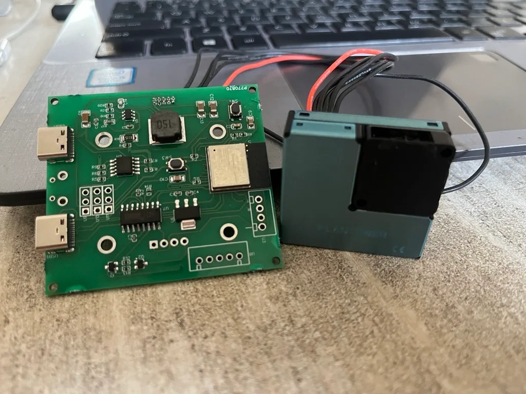
Custom Air Quality Monitor — ESP32-C3 PCB with Multi-Sensor Integration
An indoor air quality company needed a fully custom, branded monitoring device — not a relabeled sensor module. We designed a single PCB around an ESP32-C3, integrating USB-C power management, a UART interface for a laser particulate sensor, and an I2C-driven OLED display — with firmware handling sensor parsing, AQI calculation, and MQTT publishing.
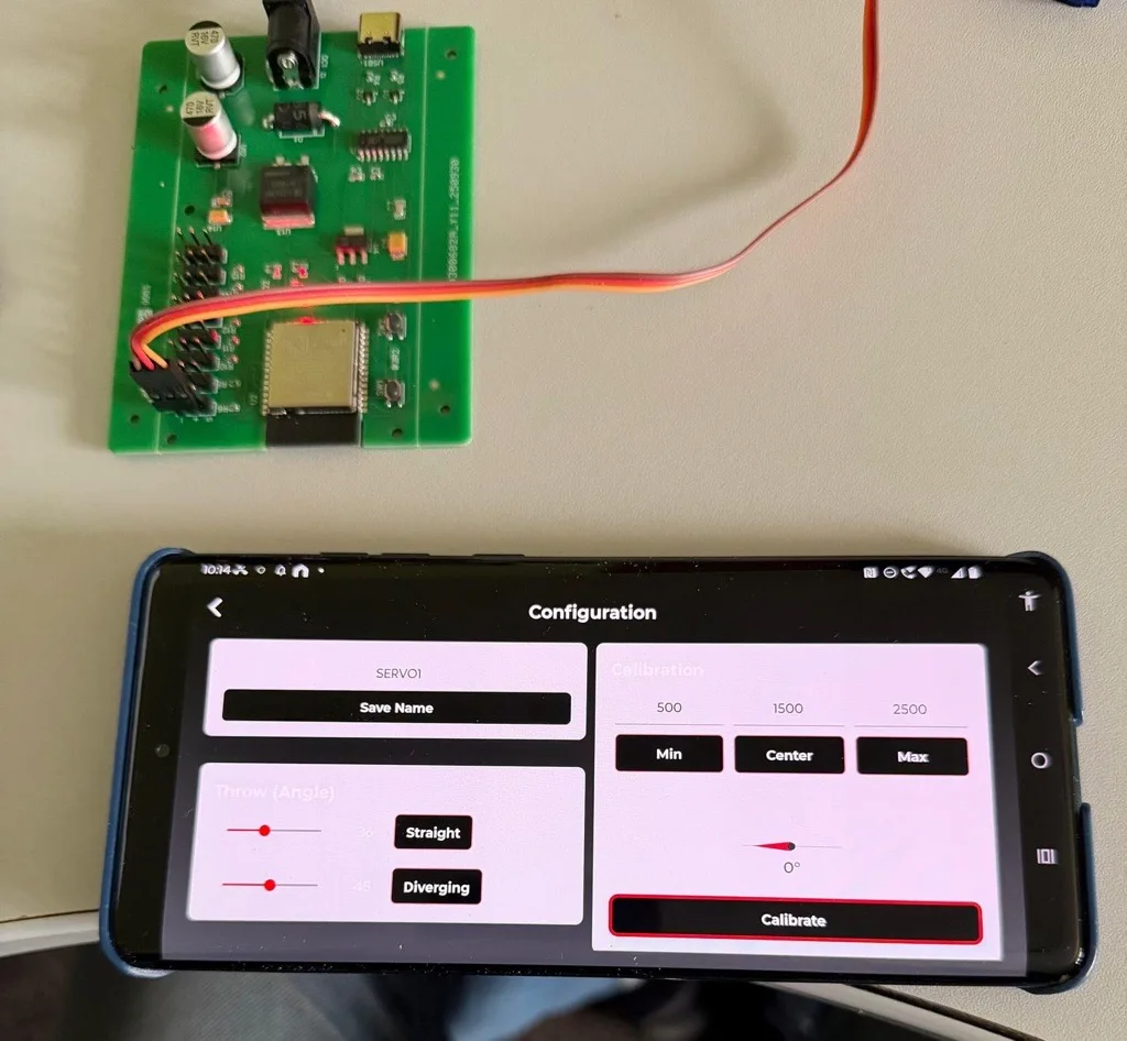
ESP32 Model Railway Track Controller — Custom Servo PCB
Eight independent servo channels per board — three boards cover 24 track points — powered over USB-C at 12V, with Wi-Fi control from a phone or tablet.
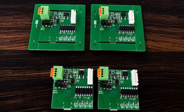
Smart Curtain Controller — Dual-Connectivity PCB, Production Run
One shared PCB behind two form factors, speaking Modbus RTU over RS485 for wired installs and MQTT for remote control — taken through a 25-unit production run with QR-coded serial traceability.
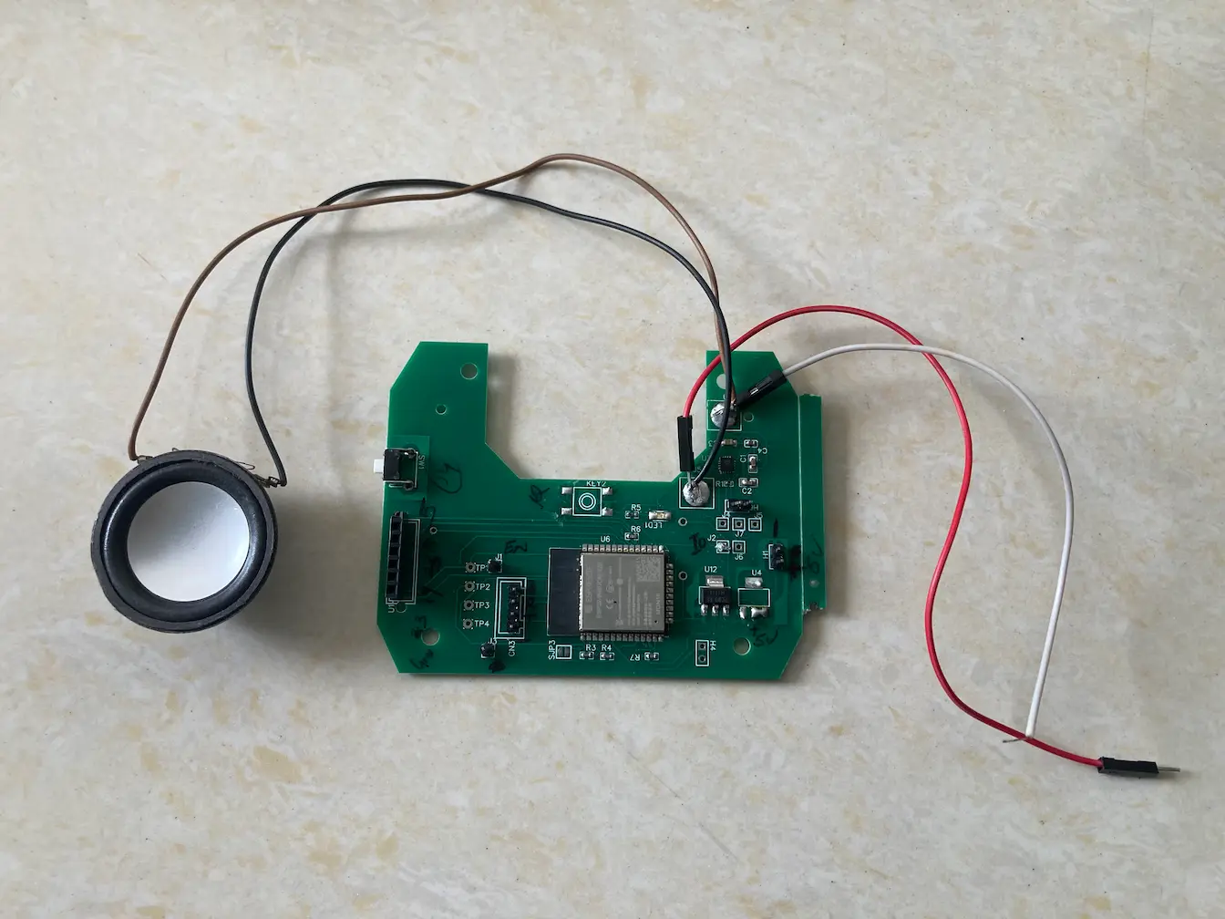
ESP32 Bible Audio Player — Custom PCB, Firmware & App
A button-press scripture audio device — custom PCB, ESP32-WROOM-32E firmware playing 365 KJV verses from internal flash, and a companion app over SoftAP Wi-Fi.
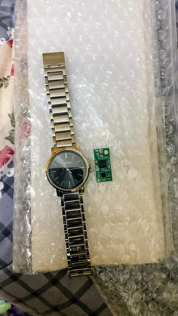
Basketball Dribble Tracker — Miniaturized ESP32 PCB
A board iterated down from a full-size ESP32-WROOM-32E dev unit to a watch-face-scale bare-die design, sized to fit inside a client-defined basketball cavity with a bleed margin.
Electronics Product Development Process
Steps overlap in practice — component selection starts during schematic design, not after — but this is the order decisions get made in.
Discovery
Understanding what the product needs to do, in what environment, at what cost.
Requirements
Electrical, mechanical, and regulatory requirements written down before design work starts.
Architecture
Block-level decisions — microcontroller, connectivity, power distribution — made before the schematic.
Component Selection
Parts chosen for availability and lead time, not just datasheet specs.
Schematic Design
Circuit captured, reviewed, and checked against requirements before layout starts.
PCB Layout
Placement, routing, and stack-up with manufacturability as a constraint from the first placement decision.
Simulation
Power supply stability, signal integrity, and thermal performance checked before fabrication.
Prototype
Small-batch fabrication of first boards — typically 3–10 units — for bring-up and testing.
Firmware Integration
Where hardware bugs that survived design review usually surface, and get fixed.
Testing
Functional testing against the requirements document — every interface, every load condition.
Validation
Environmental testing and EMC pre-compliance before committing to production tooling.
Production
Manufacturing files finalized and handed to your CM, with our team on hand for DFM questions.
Support
Available for revisions when a part goes end-of-life or a cost-down opportunity comes up.
Starting from an idea, not a schematic? We can take the project from concept through production files. Start your project →
Industries We Serve
The constraints differ significantly between these categories — part of why generic PCB layout services underperform for specialized products.
Industrial Automation
Noise immunity, wide temperature range, long product lifecycle.
IoT
Low power design, wireless coexistence, small form factor.
Medical Devices
Documentation rigor, component traceability, design controls.
Retail
Cost efficiency, ruggedness for high-traffic environments.
Smart Vending Machines
Payment system integration, connectivity reliability, uptime.
Agriculture
Outdoor durability, power efficiency for remote/solar deployment.
Consumer Electronics
Cost-down at volume, compact layout, industrial design constraints.
Automotive
Wide voltage tolerance, vibration resistance, EMC (non-safety-critical).
Energy
High-current handling, thermal management, long-term reliability.
Smart Buildings
Networked device design, BLE/WiFi/Ethernet interoperability.
Defence & Government
NDA-first engagement, ruggedized enclosure and PCB design, full component traceability — see our defence electronics design capability.
Technologies We Work With
We select the microcontroller and protocol stack based on the product's power budget, range, and data rate — not whatever's most familiar.
Microcontroller Platforms
 Arduino
 ESP32
ESP32 STM32
STM32 Nordic nRF
 NXP
NXP Raspberry Pi
For boards built around Linux-class compute, our Raspberry Pi developers bring a different set of layout and thermal considerations to the table.
Communication Protocols
 MQTT
MQTT RS-485
 MODBUS
 CANBUSESP-IoT
 Azure IoT
| Design Software | Used For |
|---|---|
| KiCad | Open-source projects, cost-sensitive engagements, full design transparency |
| Altium Designer | Complex multilayer boards, high-speed design, collaborative team workflows |
| EasyEDA | Rapid prototyping and quick-turn simple boards |
| LTspice | Power supply simulation and analog circuit verification before layout |
Dedicated Expertise
Need firmware too?
PCB design is half the product. Our embedded team writes the firmware that runs on it — same company, same accountability.
Manufacturing Deliverables
A complete package, tested before handoff — not just a layout file.
Schematics
PDF and native source files
PCB Layout
Native source files in your preferred format
Gerber Files
RS-274X, verified against fabricator design rules
BOM
Manufacturer part numbers, alternates, current availability
Pick and Place Files
For automated assembly
Assembly Drawings
Component orientation and reference designators
3D Models
STEP files for mechanical enclosure fit-checks
Manufacturing Package
Consolidated, formatted for your CM's submission process
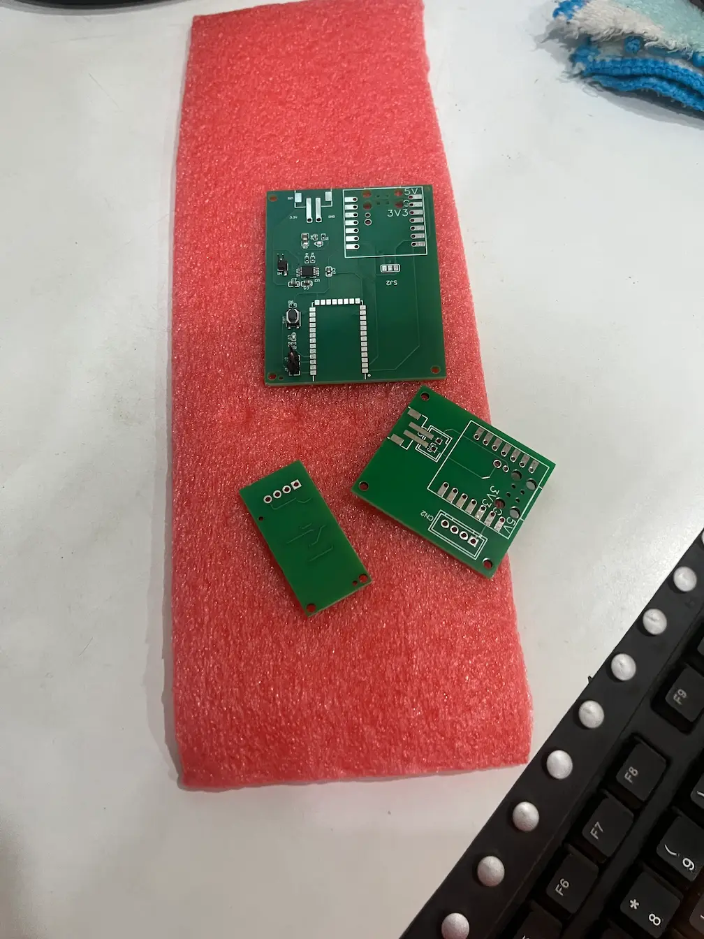
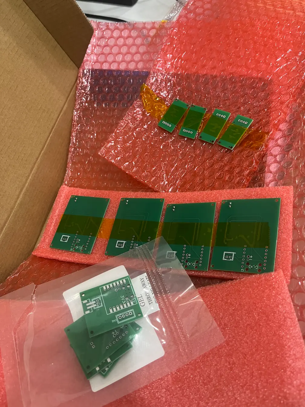
Fabricated Boards, In Hand
Bare boards from our own designs, fabricated by JLCPCB and inspected before assembly.
Why Our PCB Designs Are Manufacturing Ready
A board that works on the bench and a board ready for volume manufacturing are not automatically the same thing.
DFM
Trace widths, spacing, and via sizes checked against your specific fabricator's capability, with margin for process variation.
DFA
Component placement and orientation reviewed for automated pick-and-place, with clean courtyard clearances.
Signal Integrity
Controlled impedance, length matching, and return-path continuity on high-speed, RF, or sensitive analog nets.
EMI
Ground plane continuity and routing decisions made to reduce emissions before compliance testing, not after.
Power Integrity
Decoupling placement and plane sizing to keep supply rails stable under transient load.
Thermal Design
Copper area and thermal vias planned around actual power dissipation, not assumed adequate.
Component Availability
BOM checked against current stock and lead times at design freeze, with alternates for at-risk parts.
Lifecycle Planning
Parts weighted toward long-term availability for products expected to stay in production for years.
Why Outsource PCB Design Instead of Hiring In-House
Worth addressing directly, since it comes up in most first conversations.
| RecommendedDigitalMonk | Hiring In-House | |
|---|---|---|
| Time to Start | ✓ Scoping call this week — design begins on sign-off | ✗ Weeks to months of hiring and onboarding |
| Cost Structure | ✓ One quoted engagement, no idle bench time | ~ Fully loaded salary, benefits, and idle time between design cycles |
| Breadth of Experience | ✓ Patterns learned across dozens of boards and clients | ~ Sees only your product's problems |
| Software & Tooling | ✓ KiCad, Altium, and EasyEDA licenses already in place | ✗ Altium seat alone runs $5k+/year per engineer |
| Firmware Integration | ✓ Same team writes the firmware that runs on the board | ~ Needs a second hire or a handoff to your firmware team |
| Manufacturing Support | ✓ DFM review and CM coordination included | ~ Falls on the same engineer, on top of new designs |
| Scaling Up or Down | ✓ Engage per board — no bench to manage | ✗ Layoffs or idle time when design cycles slow |
| IP & Design Files | ✓ You own every schematic, layout, and Gerber file | ✓ Standard employment agreement |
Honest comparison — we let the facts speak
Why Companies Choose DigitalMonk for PCB Design
Laying out a board correctly is the baseline, not the differentiator. Here's what actually changes the outcome of a hardware project.
Firmware and PCB, Same Team
Pin mapping, interrupt routing, and power sequencing get decided with firmware in mind at the schematic stage — not discovered during bring-up because two separate teams never talked.
Prototype Through Production
The engineer who designed your schematic is still available when your contract manufacturer has a DFM question, or your first batch hits a yield issue six months later.
Years of Hard-Earned Lessons
Most of our layout mistakes happened on our own boards, years ago — bad return paths, end-of-life connectors, hot loops routed wrong. That experience is now baked into every design review, not relearned on your prototype.
Startup Speed, Without Skipped Steps
A bad software release gets patched. A bad PCB spin costs three weeks and real money. We parallelize what can be parallelized — sourcing while layout is underway — without cutting the checks that catch problems before fabrication.
End-to-End, One Point of Contact
No coordinating between a schematic contractor, a separate layout house, and a third firm for manufacturing files. One team, start to finish.
Manufacturing-Ready by Default
Every board is checked against DFM, signal integrity, and thermal constraints before it's called finished — not left for your CM to discover in a rejection report.
Frequently Asked Questions
Got questions before starting your project? Here are the ones we hear most.
A complete engagement typically covers schematic design, component selection, PCB layout, and manufacturing files (Gerbers, BOM, assembly drawings). Some engagements also include design review, simulation, and prototype bring-up support.
Schematic design typically takes 5–10 working days, and layout takes another 7–15 working days depending on complexity. Design review adds 2–4 days.
KiCad, Altium Designer, and EasyEDA, chosen based on project complexity and whether the files need to integrate with your existing workflow.
Gerber files, drill files, BOM with manufacturer part numbers and alternates, pick-and-place files, assembly drawings, and 3D STEP models.
Yes — high-speed design (DDR, USB, Ethernet) and RF design (WiFi, BLE, LoRa, cellular) are core parts of the service, including impedance-controlled routing and antenna placement.
ESP32, STM32, Arduino-based platforms, Nordic nRF series, and Raspberry Pi, chosen based on your product's power, connectivity, and processing needs.
Both. Engineers who handle firmware and PCB design together avoid the pin-mapping and peripheral-conflict issues that come up when the two are designed separately.
Cost depends on layer count, component count, and whether high-speed or RF design is involved. We quote after understanding your requirements — there's no single fixed price.
DFM means designing the board so it can be reliably fabricated and assembled at your target volume without excessive rework or yield loss.
Reach out with a description of your product and requirements, even early-stage. We'll scope the project on a call with a realistic timeline and cost estimate.
What Clients Say
Real reviews from real projects.


Branded ESP32 Audio PCB Design + ESP32 Firmware Tweaks
"Great work and communication. Delivered a quality product and had a positive attitude about feedback and making revisions. Appreciate it! Thank you"
4.9★★★★★out of 5 on Google ReviewsDedicated Expertise
Need the enclosure and firmware too?
PCB design is one piece of the product. Our end-to-end embedded product development service covers the board, firmware, and enclosure — one team, one point of contact.
Have a Board That Needs to Ship?
If you're evaluating PCB design partners, the fastest way to find out if we're a fit is to describe your project and let us give you a straight answer.
Realistic timeline, realistic cost, and an honest read on what's straightforward versus genuinely difficult about your board.